


A field emission scanning electron microscopy image showing a ~30 nm gold dot formed in the center of a hollow gold parent structure supported on an oxidized Si substrate. This nanostructure was fabricated by a 'molecular ruler' resist process developed to extend the range of conventional nanolithography techniques.
Acknowledgements: A. Hatzor & B. A. Mantooth.
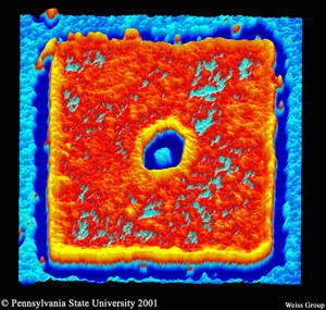
As with the previous picture, I will post the others in this series over time. To see it all now, visit the Nanotechnology Now Gallery.
"We focus on gaining atomic-scale understanding and control of materials properties. We do this by exploring, probing, and manipulating interactions and dynamics at surfaces and interfaces. We use and extend scanning tunneling microscopy to explore the surface structures, motion, and perturbations due to adsorbed atoms and molecules and due to surface features such as substrate steps and defects. We locate, study, and try to exploit the regimes in which our intuition based on macroscopic measurements breaks down. We are exploring the phenomena to be used, the ground rules, and the ultimate limits in nanometer-scale electronics and storage. Our microscopes serve not only as probes, but also allow us to manipulate matter on the atomic scale. We can thus interrogate the properties of uniquely configured atomic-scale structures. This has required the development of new tools with atomic-scale views of the surface. One new effort in our group looks at how we can bridge the gap between conventional optical microscopies and scanning probe microscopies."
—Paul S. Weiss, Professor of Chemistry, Pennsylvania State University. Weiss Group Featured Images


No comments:
Post a Comment