Tuesday, April 24, 2007

Picture of the day


Nano trees


Nano trees, Ghim Wei Ho and Prof Mark Welland


At the time this image was created, Ph.D. student Ghim Wei Ho was doing research in the lab of Prof. Mark Welland. Her project involved the fabrication and characterization of novel nanostructures. "For the remainder of my Ph.D., I will be focussing on the potential device aspects of these extraordinary structures," she said. (click to see larger version)

To see the entire series, visit the Nanotechnology Now Gallery.

Courtesy of and Copyright © Ghim Wei Ho and Prof Mark Welland, University of Cambridge Nanoscale Science Laboratory

Quote of the day

Jeff Wacker, a futurist with Plano-based Electronic Data Systems Corp., said the evolution of nanotech into the consumer arena will be marked by three phases.

"I think there's the mild, I think there's the wild, and I think there's the magical," he said.

See http://www.nanotech-now.com/news.cgi?story_id=21916

Friday, April 20, 2007

Picture of the day


Low-friction bearing assembly with two carbon allotropes

Damian Gregory Allis, Low-friction bearing assembly with two carbon allotropes


Copyright Damian Gregory Allis, Ph.D.: In this design, two diamondoid rings replace small segments of a carbon nanotube, providing a lock for a third, larger ring. The larger ring includes a stitch-work of oxygens to create an electron-rich interior whose effective circular van der Waals packing just touches that of the nanotube framework. (click to see larger version)

All images (in this series) are the result of molecular mechanics structure calculations using either Tinker (MM2 parameters) or NAMD (CHARMM). Images were made with VMD. Any inquiries concerning methods, software, or shop talk are directed to www.somewhereville.com.

To see the entire series, visit the Nanotechnology Now Gallery.

Quote of the day

"No informed person doubts that developments at the nanoscale will be significant. We debate the time-frame, the magnitude and the possibilities, but not the likelihood for large-scale change. The least-speculative views suggest that we're in for changes of an order that justifies-if not demands-our undivided attention. Will we be ready?"

~Rocky Rawstern
from an article by Matthew N. Skoufalos, April 4, 2005
http://www.rt-image.com/content=8804J05C489E548640B69C74444090441

The Weekly Roundup

Jeff Wacker, a futurist with Plano-based Electronic Data Systems Corp., said the evolution of nanotech into the consumer arena will be marked by three phases. "I think there's the mild, I think there's the wild, and I think there's the magical," he said. At the "mild" end of the scale in the next few years are lighter, stronger, frictionless and more efficient upgrades to existing materials, such as in airplane wings, solar panels and batteries.

At the "magical" conclusion, 10 years or more down the road, consumers can expect to see nano assemblers, minuscule factories using billions of molecule-size machines to build nearly any product imaginable out of a pile of raw materials.

RR: Another deep thinker who believes, as many others do, that advances in the nanosciences will lead to molecular manufacturing.

To learn more, visit: http://crnano.org/

From: Small molecules, big impact
http://www.nanotech-now.com/news.cgi?story_id=21916


Nanostellar, Inc., a leader in nano-engineered catalyst materials, today announced a first in diesel emissions technology: the introduction of gold as an oxidation catalyst. Nanostellar's NS Gold™ catalyst enables manufacturers of light- and heavy-duty diesel engines to reduce noxious emissions by as much as 40 percent more than existing pure-platinum catalysts at equal cost. Nanostellar introduced its first-generation product, based on a platinum and palladium alloy, in mid-2006, and it achieved 25%-30% higher performance than commercial pure-platinum catalysts. NS Gold™, Nanostellar's second-generation product, delivers a further 15%-20% performance increase.

RR: This is great news for the environment. As oil and gas prices rise and concern for the environment turns to action, expect to see technologies like this begin to make a difference.

From: Nanostellar Introduces Gold in Oxidation Catalyst That Can Reduce Diesel Hydrocarbon Emissions by as Much as 40 Percent More Than Commercial Catalysts
http://www.nanotech-now.com/news.cgi?story_id=21935


FriCSo, Inc., a developer and manufacturer of environmentally friendly technology and polymer-based devices that create a friction reduction nanolayer on moving parts, today announced that a test conducted by the Technion - Israel Institute of Technology found that FriCSo's Surface Engineering Treatment (SET) highly reduces particulate matter emissions, increases engine mechanical efficiency, and reduces fuel consumption.

RR: ditto my previous comment.

From: New Nanolayer-based Technology Highly Reduces Engine Emission and Improves Fuel Consumption
http://www.nanotech-now.com/news.cgi?story_id=21933


The use of nanotechnology is an innovation in the development of surface coatings, particularly in relation to UV absorbing and penetration. In meeting this challenge, Nanovations has introduced a new VOC-free technology for clear impregnating wood protection.

RR: Nanovations has recently released several new nanotech-enabled products. See http://www.nanovations.com.au/ then click on Products.

From: Nanovations introduces surface protection for woods
http://www.nanotech-now.com/news.cgi?story_id=21999


There seems to be an arms race going on among nanotechnology investment and consulting firms as to who can come up with the highest figure for the size of the "nanotechnology market". The current record stands at $2.95 trillion by 2015.

RR: An excellent article! Michael Berger debunks the hyper-hyped “trillion dollar” figures being casually thrown around. “…trillion-dollar forecasts for an artificially constructed ‘market’ are an irritating, sensationalist and unfortunate way of saying that sooner or later nanotechnologies will have a deeply transformative impact on more or less all aspects of our lives.”

From: Debunking the trillion dollar nanotechnology market size hype
http://www.nanowerk.com/spotlight/spotid=1792.php


Billionaire investor Wilbur Ross, who has made most of his money restructuring failed companies in such unglamorous industries as steel, coal, and most recently, textiles, is not the kind of guy to jump on the latest technology fad. Therefore, when someone like Ross begins investing in nanotechnology, I believe it serves as further validation that the technology is moving into the mainstream.

RR: Jack Uldrich (Access Team member -- access-nanotechnology.com/our-team.htm) sums it up nicely “My point here is that Ross is not a venture capitalist. He is a practical, experienced businessman with a great nose for turning around companies. If he's investing in nanotech, it's not because he thinks it's a fad, but because he thinks there's great value in these companies.”

From: Nanotech Wins a Convert
http://www.fool.com/investing/high-growth/2007/04/18/nanotech-wins-a-convert.aspx


"Nanotechnology could not only change our whole economy and the quality of life of Russian people, but can also drastically change all our perception about modern warfare." Sergei Ivanov, Russian first deputy prime minister
http://en.rian.ru/russia/20070419/63937318.html

Russian President Vladimir Putin has urged the government to ensure the effective spending of the major funds that will be invested in the development of nano-technologies. “This is a line of business the state will spare no effort or funds to develop,” Putin said at a conference devoted to the development of this branch of science. “The question is how to ensure this be arranged for properly and the funds be spend (sic) effectively. He said nanotechnology will lay the groundwork for new weapon systems, both offensive and defensive.

Russia is currently concentrating material and human resources to produce arm systems based on nanotechnologies, President Vladimir Putin said.
http://www.nanotech-now.com/news.cgi?story_id=22063

Russia will pour over US$1 billion (€740 million) in the next three years into equipment for nanotechnology research as it uses massive oil and gas export earnings… Ivanov predicted that 90 percent of nanotechnology developments would be used for civilian purposes and 10 percent for military purposes. http://www.iht.com/articles/ap/2007/04/18/technology/EU-TEC-Russia-Nanotechnology.php

RR: This one is pieced together from three articles. Given the thousands of scientists at large in Russia, combined with the billion dollar investment, expect to see significant progress in the nanosciences.


Since the 1960s, the best way to isolate precise instruments like atomic-force and scanning-tunneling microscopes along with fab tools from vibration was passive air tables that support weight on a cushion of air. A recent alternative is using active electronic feedback to send cancelling forces that damp out oscillations in springs.

RR: Good news on the “tools” front.

From: 'Negative stiffness' used to damp vibrations
http://www.nanotech-now.com/news.cgi?story_id=22059


A domestic water filter that uses metal nanoparticles to remove dissolved pesticide residues is about to enter the Indian market. Its developers at the Indian Institute of Technology (IIT) in Chennai (formerly Madras) believe it is the first product of its kind in the world to be commercialized. 'Based on consumption patterns of a typical Indian household, the filter is designed to have enough nanomaterials to provide 6000 litres of pesticide-free water for one year,' Pradeep said. 'After that, the company will recycle the filters to recover the silver.'

RR: At an estimated cost of £115 ($230) it may find difficulties entering the US market in any quantity. I can buy water that has been micron filtered, UV irradiated, charcoal and reverse osmosis filtered for 25 cents per gallon at the local food mart. At $230 for the filter, it would cost about $7 per gallon, which may be an acceptable figure for areas with pesticide residue problems.

From: Pesticide filter debuts in India
http://www.nanotech-now.com/news.cgi?story_id=22073


Nanoexa announced today that its subsidiary Decktron will combine technologies to develop lithium batteries that will outperform currently available batteries. The batteries could end up in plug-in electric hybrid vehicles.

RR: Yet another entry in the rapidly expanding list of companies that are vying for king of the nanotech-enabled battery market. Given the incentives (think global warming, massive pollution, and peak oil) I don’t doubt that before the dust settles there will be many more companies trying to cash in on this seemingly lucrative market.

From: High-Performance Batteries Could Solve Energy Storage Problem for HEVs
http://www.nanotech-now.com/news.cgi?story_id=22046


G24 Innovations Limited (G24i), a Cardiff -based company that aims to revolutionise solar power by leading the development of extremely lightweight, flexible solar cells, is to sponsor a competition with students from Central Saint Martins College of Art and Design to design a product that uses the company's cutting edge technology.

RR: Good news, and another indicator that alternative energy technologies are being taken seriously.

From: Cardiff sponsors solar energy contest
http://www.nanotech-now.com/news.cgi?story_id=22045


Curcumin, an element found in the cooking spice turmeric has long been known to have positive effects against certain types of cancer. Effective treatments based on curcumin however have been limited due to its poor dissolving capabilities in water based substances, leading to low absorption rates when ingested. Researchers affiliated with the Institute for NanoBioTechnology at Johns Hopkins University report to have overcome this problem by encapsulating free curcumin with a polymeric nanoparticle, creating nanocurcumin.

RR: I find it encouraging that scientists continue looking to nature in an effort to deal with one of mankind’s most deadly killers. Add “nanocurcumin” to your list of nano-things to watch.

From: Polymer Coated Curcumin Promises Effective Against Cancer
http://www.nanotech-now.com/news.cgi?story_id=22076


The ability to eliminate waste and toxins from production processes early on, to create more efficient and flexible solar panels, and to remove contaminants from water, is becoming an exciting reality with nanotechnology. This "green nanotechnology" involves designing nanoproducts for the environment and with the environment in mind.

RR: Live webcast, Thursday, April 26, 2007, 10:00 - 11:00 a.m.

From: Green Nanotechnology: It’s Easier Than You Think
http://www.nanotech-now.com/news.cgi?story_id=22051


The global search for a sustainable energy supply is making significant strides at Wake Forest University as researchers at the university's Center for Nanotechnology and Molecular Materials have announced that they have pushed the efficiency of plastic solar cells to more than 6 percent.

RR: Given the rising cost of silicon, couple with the need for alternative energy sources, efficient plastic solar cells (should they become more efficient and/or cheap) may make, as they say “plastic devices the photovoltaic of choice.”

From: Plastic solar cell efficiency breaks record at WFU nanotechnology center
http://www.nanotech-now.com/news.cgi?story_id=22027


Industrial Nanotech, Inc. (Pink Sheets:INTK), an emerging global leader in nanotechnology, announced today that it has entered into negotiations with a Fortune 100 company for the incorporation of the Company's patented nanotechnology based coating, Nansulate®, into their products. The Company estimates the value of the project to be approximately 4.5 million dollars annually once an agreement is reached.

RR: These guys are everywhere with their insulation product. Keep an eye on them as they break into new industries.

From: Industrial Nanotech, Inc. Enters Negotiations with Major Electronics Manufacturer
http://www.nanotech-now.com/news.cgi?story_id=22009


For custom reports on nanotech and cleantech news and developments, please contact me at rocky at access-nanotechnology.com

Contact me at the same address to discuss a complimentary evaluation of your project needs. Or visit http://access-nanotechnology.com/

Wednesday, April 18, 2007

Picture of the day


"Molecular Mill 1"


John Burch, Molecular Mill 1


This image is part of a presentation by the Foresight Nanotech Institute. Overall, all the images are intended to illustrate "an animated view of a nanofactory and demonstrate key steps in a process that converts simple molecules into a billion-CPU laptop computer."

Description: View of the smallest stage of the nanofactory. Wheels in upper left purify Acetylene molecules. The gray wheel at upper center presents individual molecules to the bonding tools on the white wheel at center. Hydrogen is stripped from the carbons by the white wheel at lower left, leaving only two carbon molecules. These two atoms are applied to the moving chain mechanism on the right to build small cubes of diamond.

© Copyright John Burch (click to see larger version)

Learn more at Lizard Fire Studios

To see the entire series, visit the Nanotechnology Now Gallery.

Quote of the day

RR: How do you - as scientists - help the public to understand the potential of nanomedicine? How can we - as a society - help insure that a nano-divide does not occur when it comes to distributing the benefits of nanomedicine to all?

Dr. James Baker:
Scientists need to take a lead role in educating the public about the potential for nanomedicine. By using the media to give real-life examples and visual representations of nanomaterials, we will be able to have people understand what is truly a real possibility and how it can benefit people's lives. The better educated the public are, the more supportive they will be of nanomedicine and the more rapidly we'll be able to develop nanomedicine applications. This relates to the second question. All healthcare is a societal issue that we need to deal with and the distribution of healthcare is one of the major issues our society will face as we move forward and our population ages. One of the hopes is that nanomedicines, nanobased health monitoring systems and nanodiagnostics can actually reduce the cost of healthcare to society. This will allow greater application of higher-quality healthcare to more individuals in our society, while at the same time, avoiding both the costs and pitfalls of current therapies. Let me give an example: To diagnose a tumor, we often have to use many different, expensive imaging studies, followed up by surgical procedures. If we can replace this with a nanomaterial, that could give a real-time diagnosis and allow earlier treatment of the disease before it becomes critical, we can save money in both the diagnostic and the therapeutic arena.

From: Nanotechnololgy Talk April 19, 2005
http://www.eurekalert.org/nanotalk/20050112/talk.php

Trillion $ Market

A spot-on bit of writing was posted today at Nanowerk, by Michael Berger. Michael titled his piece “Debunking the trillion dollar nanotechnology market size hype” which is just what he did.

As he pointed out “There seems to be an arms race going on among nanotechnology investment and consulting firms as to who can come up with the highest figure for the size of the ‘nanotechnology market.’ The current record stands at $2.95 trillion by 2015.” This observation has been long in coming. Too long have we blithely accepted that anything that contains the slightest amount of nanoscale material contributes as a whole to the total market. His words for this market forecast method are “…taking every product that has anything to do with nanotechnology, however miniscule or remote, adding up the entire value chain of these products, and claiming this is ‘the market for nanotechnology’...”

I think his closing puts the whole hyped issue in perspective “I guess the point I am trying to make here is that these trillion-dollar forecasts for an artificially constructed "market" are an irritating, sensationalist and unfortunate way of saying that sooner or later nanotechnologies will have a deeply transformative impact on more or less all aspects of our lives.”

Well written and informative.

Read the entire article here:
http://www.nanowerk.com/spotlight/spotid=1792.php

Tuesday, April 17, 2007

Picture of the day


Starship

John Hart, Starship


This is an image of a carbon nanotube structure (or "architechure") grown by chemical vapor deposition on a silicon substrate, by John Hart, a post-doctoral associate at MIT. Architectures are formed by self-organization of carbon nanotubes as they grow upward from a silicon substrate and a catalyst layer. If the catalyst is uniformly distributed, nanotubes grow everywhere on the substrate. How the nanotubes organize is defined by how they "push" and "pull" each other to produce the architectures. If the catalyst is only located in certain areas (patterned), then nanotubes grow only in those areas. In this image, the catalyst is patterned by photolithography, where a light-sensitive polymer is used to specify where the catalyst is placed.

Each structure consists of thousands to millions of parallel nanotubes (the density of nanotubes growing from a substrate is about 20 billion per square centimeter). The star-shaped patterns in "starship" are approximately one millimeter wide.

The image was taken using a scanning electron microscope.

Many such images, which are displayed at www.nanobliss.com, resemble everyday objects and macroscopic landscapes; however, these structures are formed by self-assembly interactions at much smaller scales.

So far, most of these images have arisen as results of normal experiments, but in some cases John took a bit more time to image the sample in the microscope, or to refine or add color to the image afterwards. John says he's still very much a scientist, but is seeing now how artistic endeavors can enhance the presentation and visualization of science, and how laboratory techniques such as fabrication and self-assembly can be a new art form.

Courtesy of and Copyright © Anastasios John Hart. Permission to reprint required.

To learn more, visit John's website and his research page

Look for the series at the Nanotechnology Now Gallery soon.

Quote of the day

According to Tom Theis, IBM's director of physical sciences, "Nanotubes with diameters of only 1.5 to 2 nanometers possess many times the strength of steel and conduct electricity as both a metal and a semiconductor." Because of these properties, Theis says, "I can't imagine a more aggressive transistor technology right now."
http://www.computerworld.com/action/article.do?command=viewArticleBasic&taxonomyName=hardware&articleId=9003397&taxonomyId=149


In the chip-making world of the future, microprocessor makers will likely use carbon nanotubes instead of transistors to make chips smaller and more powerful.

"There's a lot of work going on in carbon nanotubes and some other exotic devices which may be the next technology that takes us to new levels of speed and performance."

~Ned Barnholt, Agilent Technologies CEO
http://msnbc.msn.com/id/6713190/


"The future is bright for nanotechnology. Nanoscale processes like General Motors' quick-plastic-forming aluminum are simplifying supply chains. Nanoparticulate diagnostics from companies like Nanosphere can turn fatal diseases into livable conditions. And nanoelectronics innovations from carbon nanotube electronics to spintronics promise to keep Moore's law going for another 30 years."

~Matthew Nordan, President, Lux Research


Nanotubes have gone into warp drive. Baughman's team can churn out up to ten metres of nanoribbon every minute, as easily as pulling a strip of sticky tape from a reel. This ribbon can be up to five centimetres wide, and after a simple wash in ethanol compacts to just 50 nanometres thick, making it 2,000 times thinner than a piece of paper. The ribbons are transparent, flexible, and conduct electricity. Weight for weight, they are stronger than steel sheets, yet a square kilometre of the material would weigh only 30 kilograms. "This is basically a new material," says Ray Baughman (Director of the NanoTech Institute of the University of Texas at Dallas). http://www.nature.com/news/2005/050815/full/050815-8.html

Nanotube News Highlights

Carbon Nanotubes (CNTs) continue to hold great promise in many areas. While our understanding of the properties of CNTs has increased, and we have made some small progress towards solving the primary production and separation issues, unfortunately, for the most part, the same obstacles that were in place 5 years ago continue to stymie research and development efforts.

Purity is definitely an issue; most producers of nanotubes now sell them based on “percent pure.” The higher the purity the higher the cost, well above $1,000 per gram in many cases.

Purity is related to “what percent is nanotubes and what is impurities” as well as “what percent is a certain type of nanotube, while the remainder is another type or types.” (Note that there are three main types of carbon nanotubes and as many as 80 sub-types, each with distinct properties). Current separation techniques simply do not produce "pure enough" batches of CNTs (at a reasonable cost).

Other major hurdles include production scaling problems (and therefore cost) and functionalization (necessary for medical uses).

Another major hurdle has been, and remains, both the public perception and the actual risk associated with these vanishingly small materials; we just don’t know, yet, all the ways in which nanotubes may prove toxic.

Expect to see nanotubes play a significant role in dozens of major industries in the near future (say 3 – 5 years) provided that the usual caveats are met: low cost and high production volumes, coupled with cost-effective separation methods.

Where strength-to-weight is an important factor, expect to see nanotubes become a significant contributing factor, first in tomorrow’s advanced aerospace and military applications, and then consumer products.

There are an increasing number of nanoscale solutions to the screening, diagnosis, monitoring and treatment of disease, many of which involve functionalized nanotubes. Expect to see nanotubes play a significant role in medicine when functionalization issues are solved (basically, when we understand more fully their properties).


Here are some of the nanotube articles that have appeared in the period spanning March 29 to April 4, 2007.


The Department of Physics, Panjab University, is working on a project that could have a far-reaching impact on defense warfare. The department is trying to exploit nanotechnology to develop a material, which when used as a coating, would increase the shock absorbing capacity of the object on which it would be coated. Prof V K Jindal, faculty member of the department and in-charge of the project, said carbon nanotubes are being used to develop the material. “We are studying the properties of carbon nanotubes. The tubes are very strong and are, hence, durable. One possibility is to make a liquid that can be used as the coating substance.”

RR: At the very least, they will learn more about the properties of nanotubes, as well as how to produce them.

From: PU research on nanotechnology could impact defense warfare
http://cities.expressindia.com/fullstory.php?newsid=229446


Polynano™ carbon nanotube field emission device (CNT-FED) features perfect flat outer screen surface, flat rear screen, very thin thickness, high beam current output of carbon Nanotube emission cathode, circle phosphor dot screen anode, monochrome output, see-through type, wide-environmental operation application. Monochrome display for 32x32 resolution character and image interface application. Its use is very effective for established high visibility wording and character recognition icons.

RR: This bit is a feature on Polytron Technologies, Inc. Their CNT-FED is one of many CNT-based screen technologies. The company that brings an inexpensive and easy to mass produce screen to market will be in an enviable position.

From: Polytron Technologies, Inc.
http://www.glassonweb.com/articles/article/407/


NEC Corp has announced it prototyped a field effect transistor (FET) coating using carbon nanotube solution and achieved an on/off source-drain current (comparison of current when the power is on and off) of up to 107 by making channel length longer. Given low temperature during manufacturing process, the carbon nanotube FET coating is expected for application to flexible devices using plastic substrates.

RR: As I say above, the company that brings an inexpensive and easy to mass produce screen to market will be in an enviable position.

From: NEC Prototypes Carbon Nanotube Transistor Coating
http://techon.nikkeibp.co.jp/english/NEWS_EN/20070403/130098/


A team of University of Pennsylvania and Rice University researchers have added a significant new step to the creation of materials fortified by single-walled carbon nanotubes, or SWNTs, resulting in a nylon polymer composite with greater strength and toughness and opening the door for researchers to broadly improve the mechanical properties of such composites at the molecular level. The resulting nanocomposites with the covalent bond exhibit as much as 160 percent higher modulus, 160 percent higher strength and 140 percent higher toughness.

RR: Yet another example of where our understanding of the nanoscale will likely yield products with vastly improved characteristics. As they say “Nanotube-based composites have the potential to revolutionize fabrics, structural materials for aerospace, electrical and thermal conductors for energy applications, nano-biotechnology and other disciplines.” Perhaps an understatement given the amount of R&D investment in this area, and the well-established potential of nanotubes.

From: Seeking the Next Kevlar: Penn Researchers Fine Tune Nanotube/Nylon Composite Using Carbon Spacers
http://www.nanotech-now.com/news.cgi?story_id=21684


Researchers from the three University of Texas campuses in the Dallas-Fort Worth metropolitan area are combining their expertise in biomedical science, engineering and physical sciences on projects aimed at solving real-world medical problems. Teams receive up to $100,000 for their respective projects, which program leaders say will allow the researchers to attract additional external funding from conventional sources, such as federal agencies.

Among the funded projects:

“Fabrication and evaluation of a combined near infrared fluorescence and hyperspectral imaging system for carbon nanotube vectors" - Dr. Harold "Skip" Garner, professor of internal medicine and biochemistry at UT Southwestern, and Dr. Paul Pantano, associate professor of chemistry at UT Dallas. This project relates to the use of carbon nanotubes as sensors within living cells as well as their potential use in targeted cancer therapies.

RR: You’ll be reading a lot more about nanotube/sensor applications in the future as we learn how to functionalize the CNTs. This area holds great promise in the screening, diagnosis, monitoring and treatment of disease.

From: UT Metroplex institutions to collaborate on biomedical research
http://www.nanotech-now.com/news.cgi?story_id=21687


Despite the attractive electrical properties and physical features of single-walled carbon nanotubes, incorporating them into scalable integrated circuits has proven to be a challenge because of difficulties in manipulating and positioning these molecular scale objects and in achieving sufficient current outputs. Now, researchers at the University of Illinois, Lehigh University and Purdue University have developed an approach that uses dense arrays of aligned and linear nanotubes as a thin-film semiconductor material suitable for integration into electronic devices.

RR: This is one of many R&D efforts aimed specifically at incorporating nanotubes into electronics. Many in the know figure that nanotubes are one way that we may extend Moore’s Law past 2012-2015.

From: Linear arrays of nanotubes offer path to high-performance electronics
http://www.nanotech-now.com/news.cgi?story_id=21429


Raymor Nanotech will begin to offer in the second quarter of 2007 various high purity grades of single-walled carbon nanotubes (C-SWNT) for emerging markets. To achieve this, Raymor Nanotech launched its Purification department in 2006.

RR: Another step towards creating purified CNTs. They do not, however, state the cost, nor the volumes expected. And note that the most pure type is still not 100% pure (“the Purified Grade is a high quality SWNT product with excellent graphitization, an average length of 5 microns, and a very low metal (less than 1.1 atomic %) and amorphous carbon content”).

From: Raymor will Offer Various High Purity Grades of Single-Walled Carbon Nanotubes for Emerging Markets in the Second Quarter of 2007
http://www.nanotech-now.com/news.cgi?story_id=21558


New research published in the March 19 issue of Applied Physics Letters suggests that carbon nanotubes may soon be integrated into ever-shrinking cell phones, digital audio players, and personal digital assistants to help ensure the equipment does not overheat, malfunction, or fail.

RR: Another example of the vast potential of nanotubes. “Carbon nanotubes, however, maintain their impressive combination of high strength, low weight, and excellent conductivity, and the carbon nanotube coolers can be manufactured very cost effectively, Vajtai said.”

From: Cool Findings: Nanotubes Could Improve Thermal Management in Electronics
http://www.nanotech-now.com/news.cgi?story_id=21559


Please contact me at rocky at access-nanotechnology.com for detailed reports on this or any other "nanotech" area, including advanced materials, nanomedicine, energy, etc.

Monday, April 16, 2007

Picture of the day


Disorder

John Hart, Disorder


This is an image of carbon nanotube (CNT) structures grown by chemical vapor deposition on a silicon substrate, by John Hart, a post-doctoral associate at MIT. At first, a uniform film of CNTs - like grass growing from a field of seeds - sprouted upward from a substrate. Later, some of the CNTs arranged into groups, which grew more rapidly than their neighbors. These groups of CNTs were then constrained by a second substrate, a "cap" which is spaced above the growth substrate. The groups bent and changed direction when they ran into the cap, to give the disordered structures shown in the image. The worm-like structures in "disorder" are approximately 50 micrometers in diameter, which is just less than the width of a typical human hair.

The image was taken using a scanning electron microscope.

Many such images, which are displayed at www.nanobliss.com, resemble everyday objects and macroscopic landscapes; however, these structures are formed by self-assembly interactions at much smaller scales.

So far, most of these images have arisen as results of normal experiments, but in some cases John took a bit more time to image the sample in the microscope, or to refine or add color to the image afterwards. John says he's still very much a scientist, but is seeing now how artistic endeavors can enhance the presentation and visualization of science, and how laboratory techniques such as fabrication and self-assembly can be a new art form.

Courtesy of and Copyright © Anastasios John Hart. Permission to reprint required.

To learn more, visit John's website and his research page

Look for the series at the Nanotechnology Now Gallery soon.

Quote of the day

"Enhanced abilities to understand and manipulate matter at the molecular and atomic levels promise a wave of significant new technologies over the next five decades. Dramatic breakthroughs will occur in diverse areas such as medicine, communications, computing, energy, and robotics. These changes will generate large amounts of wealth and force wrenching changes in existing markets and institutions."

~Joseph Kennedy, Senior Economist, in a speech to the Joint Economic Committee of the United States Congress. March 2007
http://www.house.gov/jec/publications/110/nanotechnology_03-22-07.pdf

Show me the money, Pt. III

Today I will again cover what’s happening in the nano-investment world.

Here is a list of some of the noteworthy investments going to "nanotech" companies, universities, and VC funds, for period February 10, 2007 to March 9, 2007. Also covered are articles on how investments are performing.

Why did I put nanotech in quotes? Because the definition of nanotechnology remains elusive at best, and is often purposefully misapplied to fit the self-promotional goals of some companies who may not actually be working with nanoscale materials. The listings below are all "legit" nanotech.

Given the importance of investing, I will revisit this topic on a regular basis.


--Ener1 Group Completes Block Trade With Institutional Investors

Ener1 Group, Inc. (OTCBB: ENEI) announced that it sold 6.22 million shares of Ener1, Inc. common stock in a block trade with a group of institutional investors. Approximately $1.2 million of the $1.55 million proceeds will be invested in Ener1, Inc. as equity to accelerate the development of its hybrid electric vehicle (HEV) battery and fuel cell business plans.

http://www.nanotech-now.com/news.cgi?story_id=20540


--Big potential in U.K. nanotech

When Oxonica listed on the London Stock Exchange's Alternative Investment Market (AIM) in July 2005, the stock rocketed 100% within the first week of trading. Since then, it has been range bound and highly volatile between 120-180p. The stock trades at 150p today, yielding a market cap of $123 million.

http://www.bloggingstocks.com/2007/02/17/global-gains-big-potential-in-u-k-nanotech/


-- Nanotech index offers pure-play industry exposure

Mr. Braswell is the primary architect of the Newbridge Nanotechnology Index (NNIX), which was launched in June 2004. The index, which doesn’t yet have a license agreement with any investible funds, comprises 24 companies with market capitalizations of between $100 million and $1.3 billion.The index is market capitalization weighted, limiting all weightings to a 10% maximum. The key ingredient, according to Mr. Braswell, is the pure-play exposure to the nanotechnology market.

http://www.investmentnews.com/apps/pbcs.dll/article?AID=/20070219/FREE/70216039/1020


-- The Rice Alliance for Technology & Entrepreneurship Announces Partnership with The NASDAQ Stock Market Educational Foundation

The Rice Alliance for Technology & Entrepreneurship has received a grant award of $105,000 from NASDAQ to help fund the Rice Business Plan Competition (RBPC). This grant recognizes the substantial growth of the RBPC which, in just seven years, has become the largest and richest intercollegiate business plan competition in the world.

http://www.nanotech-now.com/news.cgi?story_id=20705


-- In Depth Research on Harris & Harris Group, Inc

Harris & Harris Group likes to think small. The business development company (BDC) invests mostly in startup firms developing so-called "tiny technology" -- microsystems, microelectromechanical systems, biotechnology, and nanotechnology. Shares were up 5% after the Motley Fool Rule Breakers recommendation announced it had invested $4 million as the lead investor in Xradia.

http://www.smalltimes.com/news/display_news_story.cfm?Section=WireNews&Category=HOME&NewsID=145296


-- Rensselaer Named One of America’s “New Ivies”

Rensselaer recently announced the establishment of the Computational Center for Nanotechnology Innovations (CCNI), a $100 million partnership to create the world’s most powerful university-based supercomputing center.

http://www.rpi.edu/dept/metasite/news/magazine/fall2006/at_rensselaer/01.html

-- Ecoprogress Considers Licensing New Nanotech Technology

The company has also reduced its accounts payable during February from approximately $340,000 to around $272,000. Also, the company is finalizing paperwork to close the second tranche of the $500,000 private placement. The company had already closed the first tranche for $304,050. It is expected to be oversubscribed.

http://www.nanotech-now.com/news.cgi?story_id=20711


-- NanoVic Signs Two New Agreements in $8 million BioNano Portfolio

In January, NanoVic completed the Bead NanoArray Commercial Development Agreement with Swinburne University of Technology. This agreement commits the parties to a total investment of $138,200 in cash and personnel resources. In February, NanoVic completed the SERS Commercial Development Agreement with Swinburne University of Technology and OptoTech Pty Ltd. This agreement commits the parties to a total investment of $354,893 in cash and personnel resources.

http://www.azonano.com/news.asp?newsID=3717


-- Emerging Turkish nanotech reverses brain drain

The foundations of the Turkish National Nanotechnology Research Center (UNAM) have been laid in Ankara under the auspices of Bilkent University by the Turkish State Planning Organization with a budget of $21 million.

http://www.todayszaman.com/tz-web/detaylar.do?load=detay&link=102916&bolum=101


-- Trinity College spin-out raises €800,000

Trinity college spin-out Cellix, a developer of technology platforms for the drug discovery and diagnostics industries, has completed an €800,000 investment round.

http://www.rte.ie/business/2007/0215/cellix.html


-- Major Fuel Cell Stocks in Review

Over 3-dozen fuel cell companies profiled.

http://energy.seekingalpha.com/article/27146


-- OVP VII closes on $250M hard cap

Early-stage venture capital firm OVP Venture Partners (OVP) has announced a final close on its seventh fund at $250 million, well exceeding its target of $200 million and at its self-imposed hard cap. After a first close of $207 million in May 2006, OVP accepted additional investments from two limited partners, the Meketa Investment Group in Westwood, MA, and the endowment of the College of the Holy Cross in Worcester, MA. OVP now has over $750 million in capital under management.

http://www.nanotech-now.com/news.cgi?story_id=20528


-- Trellis Bioscience Raises $10 Million in Series B Venture Round

Trellis Bioscience, Inc., a privately held biotechnology company, announced today that it has raised $10 million in a Series B Preferred Stock venture capital financing. New investor Novartis Bioventures Ltd. led the round, with the participation of additional new investors Pac-Link Bio Venture Investment Corporation and Sagamore Bioventures LLC. Previous investors, Easton-Hunt Capital Partners, LP and Morgenthaler Partners VII LP also participated in the financing.

http://www.nanotech-now.com/news.cgi?story_id=20448


-- I Love Harris & Harris

I love Harris & Harris (Nasdaq: TINY) for the little things -- the very little things, to be precise. This publicly traded venture-capital firm and Motley Fool Rule Breakers pick has been specializing in nanotechnology-related investments for more than a decade, and it remains one of the best "pure play" investments in the field of nanotechnology.

http://www.fool.com/investing/high-growth/2007/02/13/i-love-harris-harris.aspx


-- Sowing seeds for state's growth

Buried in the budget proposal Gov. Jim Doyle will present to the Legislature Tuesday night is a relatively small $2 million funding item for a new Wisconsin Venture Center. Initially, the center's focus would be on building relationships with financiers, with the aim of linking them up with business opportunities in economic areas that the governor is trying to build, such as bio-industry, biotechnology, nanotechnology…

http://www.jsonline.com/story/index.aspx?id=563997


-- Clean Energy Performing Well

America's twin desires to breathe clean air and to break its addiction to oil are accruing to the benefit of clean energy companies. The public market fund-raisings for such initiatives hit $10.3 billion in 2006, says Clean Edge. That's up from $4.3 billion in 2005.

http://www.energycentral.com/centers/energybiz/ebi_detail.cfm?id=291


-- Oxonica to invest extra 2.5 mln stg in Petrol Ofisi, Becton Dickinson ventures

Oxonica PLC said it will invest about 2.5 mln stg extra in the current year to accelerate the progress of two products developed through its strategic relationships with Petrol Ofisi and Becton Dickinson.

http://www.hemscott.com/news/latest-news/item.do?newsId=39732742463241


-- UK smallcap opening - Nanosience in demand after key milestone passed

Shares in Nanoscience took on a penny at 10-1/2 after the firm announced that its wholly owned subsidiary, Toumaz Technology had passed a key milestone.

http://www.hemscott.com/news/latest-news/item.do?newsId=39732742492291


-- New investment fund for startups

A new $10 million investment fund for early-stage startups, the Illinois Innovation Accelerator Fund, backed by state taxpayers and local investors, will be unveiled today. Funding will go not only to tech startups, such as in biotechnology, nanotechnology and life sciences, but also to companies involved in such areas as retail, consumer products and new media.

http://www.suntimes.com/business/273278,CST-FIN-seed26.article


-- Chicago's Business Leaders Collaborate to Create, Invest and Manage the $10 Million Illinois Innovation Accelerator (i2A) Fund

Today, the Illinois Innovation Accelerator (i2A) Fund, a $10 million seed-stage, for-profit investment fund, was launched with $6.4 million in capital commitment in its first closing. The fund will also invest in consumer product and retail enterprises, new-media start-ups, as well as companies in biotechnology, nanotechnology, cleantechnology and life sciences.

http://www.nanotech-now.com/news.cgi?story_id=20755


-- Liquidia Secures $16M in New Financing

Liquidia, a startup that has been without a full-time chief executive officer, has landed $16 million in new venture capital from New Enterprise Associates.

http://www.wral.com/business/local_tech_wire/venture/story/1220410/


-- Nanotechnology funding could push frontiers of technology

A partnership that will provide $4.5 million over three years towards research and development of materials-based nanotechnology was announced recently. The National Institute of Nanotechnology (NINT) along with the Mississauga-based Xero Research Centre of Canada (XRCC) and the Government of Alberta will invest funds and human resources to create a program and teams to lead the work.

http://www.itworldcanada.com/a/News/81df0a33-a88f-4b76-977e-ba034a010776.html


-- GE Cleans Up

When you invest in General Electric (NYSE: GE), you are, in many ways, investing in the equivalent of a mutual fund that is widely diversified across a number of commercial and industrial sectors, including financial services, health care, transportation, manufacturing, and energy. As such, the odds that an investment in the company will produce eye-popping returns are remote, but it does offer investors the prospect of garnering market-beating returns for the foreseeable future.

http://www.fool.com/investing/high-growth/2007/03/02/ge-cleans-up.aspx


-- For Stock Market, TGIF (March 2, 2007)

Nanotechnology player Applied Materials, Inc., which shed 47 cents, or 2.6 percent, to 17.98.

http://www.internetnews.com/bus-news/article.php/3663461


-- AES Corporation makes strategic investment in Altair Nanotechnologies

Altair Nanotechnologies Inc. (Nasdaq: ALTI), a leading manufacturer of safe, high-performance battery pack systems used in electric and hybrid-electric automobiles and stationary power systems, announced today that global power leader AES Corporation (NYSE: AES) has made a $3 million strategic investment in Altair.

http://www.nanotech-now.com/news.cgi?story_id=20948


-- Nano-Batteries That Keep On Going

In Feburary 2006, Motorola joined other high-profile investors such as General Electric and Qualcomm to provide A123 with $30 million in its third round of private-equity funding. The round raised A123's total investment to date to $62 million. In December, the U.S. Advanced Battery Consortium, a group that includes DaimlerChrysler, Ford Motor and General Motors, awarded A123 Systems a 36-month, $15 million contract.

http://www.forbes.com/finance/2007/03/06/nanotech-a123-motorola-pf-guru-in_jw_0306soapbox_inl.html


-- Harris & Harris Group Invests in Solazyme

Harris & Harris Group, Inc., announced today that it has made a follow-on investment of $500,000 in Solazyme, Inc., as part of a Series B round financing comprising both equity and debt. The financing was led by the Roda Group and included undisclosed individual and institutional investors and Harris & Harris Group.

http://www.nanotech-now.com/news.cgi?story_id=21004


-- Nano Chemical Systems Holdings to Merge With SolarDiesel

Nano Chemical Systems Holdings, Inc. (OTC Bulletin Board: NCSH), announced today plans to merge with SolarDiesel, Inc. a biodiesel manufacturing and distribution operations. The transaction has a value in excess of $100,000,000.

http://www.nanotech-now.com/news.cgi?story_id=21009


-- Xradia Raises $7 Million in Venture Capital Funding Led by Harris & Harris Group

Xradia, Inc. today announced the closing of a $7.0 million equity in a series D financing round. Major investors included Harris & Harris Group, Inc. an unnamed strategic investor and a prior round investor.

http://www.nanotech-now.com/news.cgi?story_id=21017


-- NaturalNano Closes $3.25 Million Deal – Will Use Proceeds To Develop Pleximer Product Line

NaturalNano, Inc. (OTCBB: NNAN) (FWB: N3N) a materials science company, today announced it has received a $3.25 million cash investment from Platinum Partners Long Term Growth IV and Longview Special Financing, Inc. through the issuance of Convertible Secured Notes. The transaction closed on March 7, 2007.

http://www.nanotech-now.com/news.cgi?story_id=21024


-- A Budding Solar Star?

This afternoon, U.S. Secretary of Energy Samuel Bodman is expected to formally announce the Bush Administration's Solar America Initiative -- a $148 million program designed to accelerate advanced solar electric technologies. He will do so from the headquarters of a small nanotechnology start-up company called Konarka.

http://www.fool.com/investing/high-growth/2007/03/08/a-budding-solar-star.aspx


-- NanoCoolers gets $3 million grant

An Austin company received $3 million from the Texas Emerging Technology Fund for its "refrigerator on a chip" cooling device.

http://www.statesman.com/business/content/business/stories/technology/03/09/9nanocoolers.html


For custom reports on nanotech and cleantech news and developments, please contact me at rocky at access-nanotechnology.com

Contact me at the same address to discuss a complimentary evaluation of your project needs. Or visit http://access-nanotechnology.com/

Friday, April 13, 2007

Picture of the day


Metropolis

John Hart, Metropolis


This is an image of a carbon nanotube structure (or "architechure") grown by chemical vapor deposition on a silicon substrate, by John Hart, a post-doctoral associate at MIT. Architectures are formed by self-organization of carbon nanotubes as they grow upward from a silicon substrate and a catalyst layer. If the catalyst is uniformly distributed, nanotubes grow everywhere on the substrate. How the nanotubes organize is defined by how they "push" and "pull" each other to produce the architectures. If the catalyst is only located in certain areas (patterned), then nanotubes grow only in those areas. In this image, the catalyst is patterned by photolithography, where a light-sensitive polymer is used to specify where the catalyst is placed.

Each structure consists of thousands to millions of parallel nanotubes (the density of nanotubes growing from a substrate is about 20 billion per square centimeter). The larger towers in "metropolis" are 200 micrometers wide, which is approximately the width of two human hairs.

The image was taken using a scanning electron microscope.

Many such images, which are displayed at www.nanobliss.com, resemble everyday objects and macroscopic landscapes; however, these structures are formed by self-assembly interactions at much smaller scales.

So far, most of these images have arisen as results of normal experiments, but in some cases John took a bit more time to image the sample in the microscope, or to refine or add color to the image afterwards. John says he's still very much a scientist, but is seeing now how artistic endeavors can enhance the presentation and visualization of science, and how laboratory techniques such as fabrication and self-assembly can be a new art form.

Courtesy of and Copyright © Anastasios John Hart. Permission to reprint required.

To learn more, visit John's website and his research page

Look for the series at the Nanotechnology Now Gallery soon.

Quote of the day

"Nanoscience will eventually revolutionize and impact upon every single aspect of our lives, including the arts. It brings all the sciences together at the level of the atom. It is completely new in the way we fabricate and make things."

~James Gimzewski, UCLA chemistry professor and nanoscience pioneer.


"If I had to pick the No. 1 challenge facing nanotechnology firms, it's environmental, health, and safety regulation and the question of public perception."

~U.S. Senator Ron Wyden (D-OR)


"Most nanotechnology-based products pose little chance for public exposure and therefore pose little risk to health or the environment. That's because most uses are in composites in which the nanoparticles are encased in a product, such as golf clubs or car bumpers, or in nanoscale structures that are part of larger devices such as electronic circuits."

~E. Clayton Teague, Director, Federal National Nanotechnology Coordination Office (NNCO)

The Weekly Roundup

Here are some of the news bits that caught my eye this week:

Students from the competition's NanoFresh group had their own innovative ideas. The team presented a water purifying mechanism designed for backpackers, travelers and commercial facilities such as schools and offices. According to team member Lyle Kaplan-Reinig, a fourth-year chemical engineering major, the group's goal for the product was for it be an easy-to-use household mechanism that eliminates harmful carcinogenic compounds found in tap water.

The first-place winner of the final competition will receive $10,000 to start up their business. Another $23,000 will be given out for the various other prizes.

RR: This is a great way to generate the next batch of technologies and products. Enable our country’s best and brightest young minds with a little cash incentive. While the dollar amounts are low, they do serve as an incentive, and are, at the very least, a step in the right direction. Anything we (the previous batches of "young minds") can do that serves to set free these young minds will be to our benefit.

From: Contest Finalists Display Inventions
http://www.dailynexus.com/article.php?a=13762


It’s a big feat of the tiniest proportions. Simon Fraser University’s Nano Imaging Lab has produced the world’s smallest published book. At 0.07 mm X 0.10 mm, Teeny Ted from Turnip Town is a tinier read than the two smallest books currently cited by the Guinness Book of World Records.

RR: This latest nanotrek (an adventure into the nanoscale) serves to illustrate our ever-expanding ability to control the nanoscale.

From: Nano lab produces world’s smallest book
http://www.sfu.ca/mediapr/news_releases/archives/news04110701.htm
image here: http://www.nanowerk.com/news/newsid=1773.php


Deformable, spherical aggregates of metal nanoparticles connected by long-chain dithiol ligands self-assemble into nanostructured materials of macroscopic dimensions. These materials are plastic and moldable against arbitrarily shaped masters and can be thermally hardened into polycrystalline metal structures of controllable porosity. In addition, in both plastic and hardened states, the assemblies are electrically conductive and exhibit Ohmic characteristics down to 20 volts per meter. The self-assembly method leading to such materials is applicable both to pure metals and to bimetallic structures of various elemental compositions.

RR: Yes, I know, that paragraph is a mouthful. What it means to me is that once again we’ve discovered a new way to create materials that may enable a whole new range of products. Harkening back to The Graduate, the phrase "I just want to say one word to you -just one word. ‘Plastics’" comes to mind, only this time with a nanotech twist. Our understanding of the nanoscale, and the often-unique phenomena found there, is looking more and more likely to enable a new generation of plastics. This news bit is just one of many recent articles that supports that assumption.

From:
Plastic and Moldable Metals by Self-Assembly of Sticky Nanoparticle Aggregates
http://www.nanotech-now.com/news.cgi?story_id=21888


The stretching alignment technique is applicable to a broad range of SWNT experiments where orientation is important, particularly in optics. The work should further our current understanding of how nanotubes interact with light, with important practical applications in optical sensing and the manipulation of individual nanotubes using electromagnetic fields.

RR: Getting nanotubes to do what we want remains one of the main logjams in commercializing products that incorporate them.

From: Stretching exercises shed new light on nanotubes
http://www.nanotech-now.com/news.cgi?story_id=21886


NCR Corp. is spinning off a new company that is developing a technology capable of combating the counterfeiting of cash, pharmaceuticals and military parts, the new company's CEO said Thursday.

Prime is developing a nano-technology that has its origins in NCR labs, Ricci said. Essentially, the process — known as LumID or luminescent identifier — creates very tiny glass beads with "chemical tags" allowing whatever has been embedded with the beads to be accurately identified, he said.

RR: Anti-counterfeiting may prove to be one of the nanotechnologies that brings greater public acceptance to an often contentious yet unrelated group of advanced technologies. Several stridently vocal anti-technology groups have been tarring all nanotechnologies with the same brush, effectively and unfairly equating those that may have downsides to all others.

From: NCR spins off company to combat counterfeit cash
http://www.nanotech-now.com/news.cgi?story_id=21883


Civil Society-Labor Coalition issues an open letter to the international nanotechnology community at large:To All Interested Parties:We, the undersigned, submit this open letter to the international nanotechnology community at large. We are a coalition of public interest, non-profit and labor organizations that actively work on nanotechnology issues, including workplace safety, consumer health, environmental welfare, and broader societal impacts.

RR: The Civil Society-Labor Coalition weighs in on the latest proposal by DuPont Chemical Company (DuPont) and Environmental Defense (ED) for "a voluntary ‘risk assessment’ framework for nanotechnology." Yes, they do make some good points, such as "Nanotechnology’s rapid commercialization requires focused environmental, health and safety research, meaningful and open discussion of broader societal impacts." However, saying "We strongly object to any process in which broad public participation in government oversight of nanotech policy is usurped by industry and its allies" is putting the cart before the horse; why does the DuPont/ED framework necessarily mean that broad public participation will go by the wayside? Of course it doesn’t, and there are efforts, here and abroad, to engage the public (visit www.nanotech-now.com/preparing-for-nanotechnology.htm to read about some of them). Are those efforts enough? I don’t know, and neither (I suspect) does the Civil Society-Labor Coalition.

From: Activist groups reject DuPont-ED nanotechnology risk framework
http://www.nanotech-now.com/news.cgi?story_id=21875


Mihail Roco, the National Science Foundation's senior advisor for nanotechnology and key architect of the National Nanotechnology Initiative, visited Rice's Center for Biological and Environmental Nanotechnology (CBEN) this spring for a three-day conference on nanotechnology-enabled water treatment. During his visit, Roco discussed the conference, CBEN and the future of U.S. nanotechnology with Rice News' Science Editor Jade Boyd.

RR: This bit goes to illustrate a beneficial use of one nanotechnology; the treatment of water. I recommend this article be read in full. Roco doesn’t sugar-coat the need to prepare for potentially negative environmental effects, and in fact, he’s speaking at the leading R&D center that was created just for that purpose, and talks about the need to prepare.

From: The future of nanotechnology
http://www.media.rice.edu/media/NewsBot.asp?MODE=VIEW&ID=9459&SnID=193827417


The year is 2027 and you're feeling decidedly unwell. Suspecting something a little more sinister than a common cold, your GP takes a sample of your saliva with a small dipstick-shaped implement coated in sensitive high-tech nanoparticles.

The colour change of the nano-particles instantly identifies the nature of the problem. The bad news is that you have a potentially debilitating genetic disease. The good news is that your doctor can quickly prescribe a customized treatment: several billion specialized nanoparticles which will enter your bloodstream and modify the offending gene at the molecular level.

RR: This ties in nicely with my "Interview with NanoTumor Center" – see (1), and "Nanomedicine at Johns Hopkins" – see (2), and "Nanomedicine Today" – see (3). And don’t be surprised to see these and other "nanomedicines" well before 2027.

From: Nano scientists make huge advances
http://www.nanotech-now.com/news.cgi?story_id=21853

(1) http://nanoscale-materials-and-nanotechnolog.blogspot.com/2007/03/interview-with-nanotumor-center.html
(2) http://nanoscale-materials-and-nanotechnolog.blogspot.com/2007/03/nanomedicine-at-johns-hopkins.html
(3) http://nanoscale-materials-and-nanotechnolog.blogspot.com/2007/01/nanomedicine-today.html


In order to assist high school students to think about the future with nanotechnology the Clarion University nanotechnology program and the art department are sponsoring a digital art contest, "Nanotechnology and the Environment for High School Students."

"The contest asks students to digitally illustrate what they think the future of nanotechnology and the environment hold. What will the effect of nanotechnology be on the environment? Will it solve our pollution and climate change problems or create environmental disasters undreamed of before? Only student creativity can tell us."

RR: This is one way to gauge public perceptions regarding nanotech.

From: Clarion University sponsors nanotechnology digital art contest
http://www.nanotech-now.com/news.cgi?story_id=21796


Venture capitalist, scientist and newsletter advisor, Josh Wolfe - in The Forbes/Wolfe Nanotech Report - looks at two favorite buys in the sector. In this case, he is selecting stocks that make the high-tech tools needed by researchers involved in nanotech.

RR: Who is making money in nanotech in these early days? Tool makers, of course.

From: A trio of experts looks at nanotech
http://www.nanotech-now.com/news.cgi?story_id=21791


Starpharma Holdings Limited makes and develops its products using nanotechnology. Its main drug is called VivaGel, a gel-based microbicide designed to protect women from sexually transmitted diseases, including HIV. The gel has made it through Phase 1 clinical trials, and the United States Food & Drug Administration (FDA) has even granted the drug fast-track status — and fast-track designation is nothing to scoff at.

RR: Great news, both in terms of a product that holds huge potential, and for the fact that it has received fast-tract status (meaning that the approval process could take a decade or more less time).

From: Starpharma Holdings Limited’s VivaGel on the Fast Track to the Market
http://www.nanotech-now.com/news.cgi?story_id=21785


The Deal's Tech Confidential was released last week and profiled five clean technologies that venture capitalists are showing increased interest in. Here's a quick rundown on those technologies and some venture-funded startups working in each area…

RR: Another positive indicator that clean technologies are starting (finally!) to garner the investment attention they deserve. Does anyone really not understand that we need more than one solution to all the problems generated by our use of and addiction to foreign oil?

From: 5 clean technologies drawing intense VC interest
http://www.nanotech-now.com/news.cgi?story_id=21770


For custom reports on nanotech and cleantech news and developments, please contact me at rocky at access-nanotechnology.com

Contact me at the same address to discuss a complimentary evaluation of your project needs. Or visit http://access-nanotechnology.com/

Wednesday, April 11, 2007

Picture of the day


CS2 on Au{111}

Wise Group, Penn State, CS2 on Au


"Surfing a wave" - CS2 riding an electronic surface state on Au{111} 236 Ã… x 236 Ã…, image of 0.2 ML CS2 on Au(111) at 4 K (Vtip = + 0.5 V, I = 200 pA). (click to see larger version)

Image by: E. H. Sykes & P. Han.

"We focus on gaining atomic-scale understanding and control of materials properties. We do this by exploring, probing, and manipulating interactions and dynamics at surfaces and interfaces. We use and extend scanning tunneling microscopy to explore the surface structures, motion, and perturbations due to adsorbed atoms and molecules and due to surface features such as substrate steps and defects. We locate, study, and try to exploit the regimes in which our intuition based on macroscopic measurements breaks down. We are exploring the phenomena to be used, the ground rules, and the ultimate limits in nanometer-scale electronics and storage. Our microscopes serve not only as probes, but also allow us to manipulate matter on the atomic scale. We can thus interrogate the properties of uniquely configured atomic-scale structures. This has required the development of new tools with atomic-scale views of the surface. One new effort in our group looks at how we can bridge the gap between conventional optical microscopies and scanning probe microscopies."

~Paul S. Weiss, Professor of Chemistry, Pennsylvania State University. Weiss Group Featured Images

To see the entire series, visit the Nanotechnology Now Gallery.

Important Quotes

Over the past 8+ years I have been gathering quotes that have a bearing on nanotechnology. Be they on investments, the ethics of advanced technologies, or forecasts and predictions, I have collects thousands of relevant quotes from individuals in business, government, academia, and the private sector.

Recently I put together a series of these quotes for my Access Team website "To help convey the most critical notions and core assumptions about nanotechnology and molecular manufacturing..." including these:

"As an emerging science in its infancy, nanotechnology promises the nano-scale manufacture of materials and machines made to atomic specifications. The impact of nanotechnology on our way of life is widely believed to reach profound and hitherto unimagined levels in the coming decades. Proposed changes include clean abundant energy, pollution-free and inexpensive production of superior defect-free materials, complete environmental restoration and cleanup, safe and affordable space travel and colonization, and quantum leaps in medicine leading to perfect health and immortality. As a result of these advances, we anticipate the obsolescence of nearly all of today's industrial and economic processes by the first half of the new century, leading to global and radical changes in life style, finance, law, and politics."

~Behfar Bastani and Dennis Fernandez
From Intellectual Property Rights for Nanotechnology

Starting around 2010, workers will cultivate expertise with systems of nanostructures, directing large numbers of intricate components to specified ends. One application could involve the guided self-assembly of nanoelectronic components into three-dimensional circuits and whole devices. Medicine could employ such systems to improve the tissue compatibility of implants, or to create scaffolds for tissue regeneration, or perhaps even to build artificial organs."

~Mihail C. Roco, Senior adviser for nanotechnology to the National Science Foundation and a key architect of the National Nanotechnology Initiative

"Over the next ten years, the fields of chemistry, physics, material sciences, biology, and computational sciences will converge in a way that will define nanotechnology and impact almost every industry, including computers, semiconductors, pharmaceuticals, defense, health care, communications, transportation, energy, environmental sciences, entertainment, chemicals, and manufacturing. Previously distinct disciplines will also combine: medicine and engineering, law and science, art and physics, etc. This merging will result in developments that are not simply evolutionary; they will be revolutionary."

~Jack Uldrich & Deb Newberry

Read this collection in full, here:
www.access-nanotechnology.com/quotes.htm

Visit Nanotechnology Now (nanotech-now.com) to read new quotes each week (left column, home page)

Tuesday, April 10, 2007

Picture of the day


Graphite nanoparticles

Cris Orfescu, Graphite nanoparticles

Image derived from black and white Scanning Electron Microscope images that was digitized and computer painted. (click to see larger version)

Learn more at Cris Orfescu's Premiere Artist Portfolio (RR: This is another of my favorites.)

NANOART - Limited edition prints. Nano-dimensional features of different materials are revealed with an electron microscope after samples have been previously prepared. The image is created by electrons (electric charged particles) rather then photons (particles of light) as in photography. The black and white electron microscope image is digitally processed, computer painted and manipulated, and printed with archival inks on fine art archival paper or canvas - contact the artist for details. All prints are signed and numbered by the artist.

To see the entire series, visit the Nanotechnology Now Gallery.

Quote of the day

"Nanotech is where breakthroughs are likely. Forget about just the cancer-detection and other advanced medical tools it's midwifing and the next-gen consumer electronics such as super-bright displays. On a planet that's on the cusp of catastrophic climate change, nano-engineered materials have the potential to make a real difference. Imagine solar power cells that are far cheaper and more efficient; batteries that allow for more efficient electric cars; components that make cleaner coal-fired power plants. These and other applications are hardly trivial--they'll save energy, reduce pollution, and maybe go a little way to making sure Times Square won't be under water for the next millennium celebration."

~David Talbot, Technology Review
http://www.technologyreview.com/blog/posts.aspx?id=17430

Interview with Norm Wu

Today, I would like to present an interview that I did with Norm Wu
Managing Director, Alameda Capital.

RR: What is your definition of nanotechnology?

At Alameda Capital, we view nanotechnology as the commercialization of technology that takes advantage of unique phenomena that exist at the atomic and molecular scale, giving rise to new and useful properties at the macro scale. Examples of such phenomena might include surface effects (such as what you get when nanoscale fibers repel liquids by changing the surface tension of a fabric), molecular forces (such as the Van der Waals forces that provide the potential for next generation non-volatile semiconductor memory based on the natural attraction of closely spaced nanowires with one another), thermal vibration (such as selectively directing thermal vibration energy to harmful bacteria to break them down), or quantum effects (which will someday enable high performance quantum computing). Commercialization is the key word that differentiates real nanotechnology from nanoscience (which is basic research at the nanoscale).

Our investments will be in the traditional market sectors of IT, life sciences and energy where the convergence of multiple technologies, including advanced materials, creates an opportunity for new companies that can integrate such multiple disciplines to capture share with a proprietary set of products. We call this "convergent technologies." Many, but not all, of these opportunities will stem from nanotechnology.

RR: As things stand today, which nanotechnologies will you likely invest within the next five years, and why?

We are currently excited about a number of sensor and imaging technologies for security and medical diagnostics, new display technologies, next generation semiconductor devices (first memory and later logic), and certain alternative energy technologies. Each of these have large existing markets, reasonable capital requirements, good technology maturity, and talented entrepreneurs who have developed a compelling value proposition based on the convergence of nanotechnology with other technologies.

RR: Overall, what do you like about nanotech as an investment area?

Nanotechnology, if commercialized on a timely basis, has the potential to transform large existing markets. It's usually not about creating new markets, although there is some potential for that too. Nanotechnology also provides a great opportunity for start-ups to capture market share from existing competitors by being smart about how they integrate nano and other technologies to create compelling new properties resulting in such products as low cost/ultra-sensitive medical imaging, low energy high brightness displays, ad hoc wireless sensor networks, high density memory storage, low cost photovoltaics and more.


Read the entire interview, here:
www.nanotech-now.com/products/nanonewsnow/issues/017/017.htm#Wu

Monday, April 9, 2007

Picture of the day


20x20um organic film, cc mode


Pacific Nanotechnology, 20x20um organic film, cc mode


Pacific Nanotechnology provides products and services that facilitate advances in nanoparticle technology and research. Our products are optimized for research, development, and process control applications when visualization, modification, and measurement of nanoparticle or nanopowder is critical.(click to see larger version)

To learn more about and to see more of these images, check out the following pages:

Pacific Nanotechnology Nanoparticle Image Gallery AFM images of nanoparticles, AFM data of nanopowders, AFM images of thermoplasitc elastomer, carbon nanotubes, polysterene particles, polymer particles, quantum dots, QD, latex spheres, drug powder, drug crystallines, polished quartz,blood cells, CNT, DNA, sol-gel, inclusions, triblock co-polymer, colloids, colloidal gold, colloidal gold spheres, carbon black, polypeptides, calcium phosphate, CaP, etc.

Pacific Nanotechnology Nanoparticle Technology

To see the entire series, visit the Nanotechnology Now Gallery.

Quote of the day

"The successful companies will be those that can commercialize innovations that merge biotechnology, infotechnology, cognitive intelligence and nanotechnology."

~Robert McMahan, Ph.D., S enior Advisor to the Governor of North Carolina for Science and Technology www.nanotech-now.com/news.cgi?story_id=21257

Plasma Gasification

The facts
America generates 245 million tons of municipal solid waste every year, a figure that continues to grow.

The problem
Landfills are filling up, land is no longer easily available, and toxic chemicals leach into the soil and water table. In addition, landfills and incineration are becoming regulatory, socially and environmentally unacceptable.

The technology that may cure the problem
Plasma gasification (PG) -- Turns trash into clean energy and produces salable fuels, valuable metals and silicates, and chemicals for plastics. It is capable of breaking down almost any material--right down to its constituent elements--except for nuclear waste.

One of the companies with the potential solution is the Startech Environmental Corporation (www.startech.net -- OTC Bulletin Board: STHK -- http://finance.yahoo.com/q?s=sthk.ob&d=t) (the remainder of this article is about Startech and their process, unless otherwise stated)

How it works
Waste materials, including hazardous and nonhazardous solids, liquids and gases, are fed into a chamber (the Plasma Converter) where they are subjected to a plasma arc. “The arc in the plasma plume within the vessel can be as high as 30,000 degrees Fahrenheit ... three times hotter than the surface of the Sun. When waste materials are subjected to the intensity of the energy transfer within the vessel, the excitation of the wastes' molecular bonds is so great that the waste materials' molecules break apart into their elemental components (atoms). It is the absorption of this energy by the waste material that forces the waste destruction and elemental dissociation.” (1)

By-products are synthetic gas (“syngas” AKA: Plasma Converted Gas or PCG) and “an obsidian-like stone, which is non-toxic and non-leachable” that can be used as a raw material for other products for the construction and abrasives industries.

The process also generates more electricity that it consumes; the PCG can be used to generate steam that in turn can drive a generator or turbine that produces electricity, or to make hydrogen or methanol.

Some of the waste stream products that may benefit the most (those that are the hardest or costliest to dispose of or are the most toxic [*]) include:

 Medical waste
 Outdated pharmaceuticals
 PCBs
 Chemical agents
 Hazardous incinerator ash
 Various biological wastes
 Sludges
 Paints and solvents
 Electronic industry waste
 Contaminated soils
 Asbestos

[* current disposal costs are approximately $900 to $2,000 per ton, and rising]
(2)

Who else has similar technology?

Renewable Energy Technologies (www.cogeneration.net/plasma_gasification.htm)
Geoplasma (www.geoplasma.com)
Recovered Energy (www.recoveredenergy.com)
PyroGenesis (www.pyrogenesis.com)
EnviroArc (www.enviroarc.com)
Plasco (www.plascoenergygroup.com)
Safe Waste And Power (www.safewasteandpower.com)
and others

Who is funding it or has invested in it? Among others:

Cornell Capital Partners, L.P. (Sept. 19, 2005: “up to $20 million of funding in the form of a Standby Equity Distribution Agreement (SEDA) to be drawn down incrementally over a 24-month period at Startech's sole discretion.”)
The Department of Energy (DOE) (Aug. 3, 2005: “$500,000 for further demonstrations of the Company's StarCell Hydrogen system … to demonstrate the production of hydrogen from Municipal Solid Waste.”)

Markets

Municipalities that are running out of landfill space
Businesses and municipalities that need to comply with existing and future environmental regulations regarding landfills and incineration
Businesses looking for alternatives to fossil fuels
Municipalities looking for ways to meet power needs

Potential drawbacks

There has been concern by environmental groups that the “obsidian-like stone” may contain heavy metals that could leach into groundwater. Startech states that “No hazardous organisms or agents that go into the Plasma vessel survive” (3) and that the “stone” is non-toxic and non-leachable.

The up-front costs of up to hundreds of millions of dollars will be hard for many municipalities to swallow, despite the advantages inherent in the technology.

David J. Phillips (10Q Detective) sounds several cautionary notes, here http://smallcap.seekingalpha.com/article/27196

Upsides (according to Startech)

Generates more electricity than it consumes
Eliminates the need for new landfills and incinerators
Could empty out existing landfills and return the land to other uses
Could also process bio-hazards such as anthrax

The cost

A $250 million Startech Plasma Converter can handle approximately 2,000 tons of waste per day, an amount that is roughly what a city of 1 million people produces. It is estimated that the cost could be recouped in around 10 years, given today’s dumping fees. And when you consider that the system is capable of generating more electricity that it consumes, as well as the PCG, the payoff could come much sooner.

What may it replace? (Who will it put out of a job or cost money?)

Landfill operators who will loose revenues.

What may it enable?

It appears that the Startech “Starcell” has promise (the Company's hydrogen-selective membrane filter that separates hydrogen from the PCG). As there are no harmful by-products, and hydrogen can be produced from traditional waste streams, this technology may be one of several that helps enable a hydrogen economy.

Who is using it now, or will be in the near future?

The City of Chitre, Panama (a 200 ton per day PC facility)
The City of David, Panama (a 200 ton per day PC facility)
The City of Las Tablas, Panama (a 200 ton per day PC facility)
[all three intended for “processing municipal solid waste and producing ‘green electrical power.’”]
GlobalTech Environmental Corporation, a Chinese corporation (a 20,000 pounds per day PC facility, intended for processing PCBs Polychlorinated Byphenyls) and POPs (Persistent Organic Pollutants))
Future Fuels, Inc., (FFI) (a 100 ton per day PC facility, for a Waste-to-Ethanol Facility)
Mihama Incorporated (a 5 ton per day PC facility, for PCBs and PCB contaminated materials)
PlasTech Solutions, Ltd., Australia. (a 10 ton per day PC facility, for industrial and institutional wastes)
Ercole Marelli HiTech srl of Milan, Italy (contracts for “more than $40 million”)
And many more – see www.prnewswire.com/gh/cnoc/comp/113537.html and the press from the other companies listed above.


Disclaimer: I am not a stock analyst and this is not a suggestion to buy or sell stock in any of the companies mentioned, nor do I own stock in any of them.

Note: this is one of many of the types of reports we do for our clients at access-nanotechnology.com

(1) http://www.startech.net/plasma.html
(2) http://www.startech.net/overview.html
(3) http://www.startech.net/faqs.html
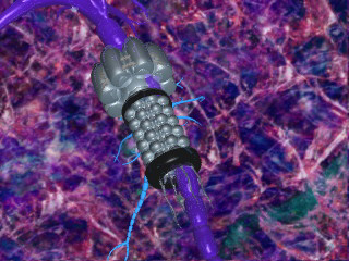
Thursday, April 5, 2007

Picture of the day


"Nano-biodevice"

Charles Ostman, Nano-biodevice


Courtesy of and Copyright © Charles Ostman: This is a 3D rendering of a theoretical neural repair "nano-biodevice", reconstructing the insulating outer membrane of a damaged neural axon. Like the "neural interface biochip" this is a slide extracted from the animation. This animation was eventually shown at SigGraph, on PBS televsion, and has been incorporated in related content for events in the US, Europe, and Asia.

Special thanks to Kevin Cain, then the director of computer graphics animation at AAC, and the spectacular efforts of over 30 students and fellow instructors who worked for approx. 9 months to create this production. Rendered in Maya 3D, and a variety of other rendering applications.

Visit his Evolution into the Next Millennium site.

To see the entire series, visit the Nanotechnology Now Gallery.

Quote of the day

"Nanotechnology is about to dramatically change virtually every aspect of how we work, live, and play; in fact the process has already begun. If you've used a UV-blocking sunscreen it may well be 'powered' by nanospheres of titanium dioxide - the opaque stuff of lifeguards' noses - which, in its nano form, happens to be transparent to visible light, but not to UV. Similarly, nanospheres in your toothpaste are (or will soon be) giving you that ultra-bright smile. And Berkeley Lab's 'Materials Sciences Division' has recently demonstrated how to use a new electro-thermal technique on carbon nanotubes to turn them into 'conveyor belts' that move individual atoms to precise targets, potentially forming the basis for far more efficient nanoscale manufacturing."

~Jeffrey R. Harrow, author of The Harrow Technology Report. From: http://www.futurebrief.com/jeffharrownanolife022.asp

Interview with FEI's Mike Thompson

Today, I would like to present an interview I did with Mike Thompson, Business Development Manager, Nanotechnology at FEI Company.

RR: "Nanotechnology" is an oft-abused term; what definition do you use?

Your oft-abused comment is justified as the term "Nanotechnology" has a chameleon quality and shifts according to the environment in which it is placed; now as our awareness of Nanotech becomes mature we need to be more specific.

The interest and considerable investment associated with the nanotechnology rests in the fact that there is a transitions zone in the properties of matter as one shifts from atoms to bulk materials. The zone in which properties change rapidly is in the linear dimensional range of approximately 1nm to 100nm, this range is often quoted in definitions. As range is an approximation we can capture its meaning by using the term "nanoscale". The objective of nanotechnology is new, and is to functionalize this size/shape property dependence of nanoscale matter. This approach differs from past, current and future engineering which has the objective of functionalizing the "invariant properties" of bulk matter.

Many definitions of "Nanotechnology" are misleading as they can include "science" as a component of the definition. This is at best a convenience as much of what we read about today relates to science at the nanoscale. Here we should emphasize that nanoscale research is essential work as we cannot efficiently functionalize events at the nanoscale until we can understand, and characterize, their properties. The amount of research and engineering which is required to commercialize Nanotechnology is a huge undertaking and has probably been underestimated. While science is a precursor to the creation of a potential product, the contribution is one of the enablement and as should not be incorporated in the definition of "Nanotechnology."

RR: By your estimation, how large (in terms of $US) is the nanotech tools market today? How does that compare to 10 years ago, and how will it compare to 10 years from now?

In 1995, the "nanotools" market was under $US 300 Million US. The total Nanotech tools served available market in 2005 was close to $US 1 Billion. Market growth is expected to be roughly 14% per year through 2008. Predictions beyond this point are speculative and will depend upon the rate of adoption rate of tools by industry as nanoscience-based products move from prototyping through to production.

Read the entire interview, here:
http://www.nanotech-now.com/products/nanonewsnow/issues/034/034.htm#main

Wednesday, April 4, 2007

Picture of the day


"Nanorobot in the bloodstream"

Svidinenko Yuriy, Nanorobot in the bloodstream

Courtesy of and Copyright © Yuriy Svidinenko (click to see full sized version)

Yuriy Svidinenko: In this study I'll try to simulate simple mobile cell-repair nanorobot and try to analyse some of it's subsystems. Here, I want to focus on the purely simulation aspects of the cell repair nanorobot's functions and parts.

See Cell Repair Nanorobot Design And Simulation for details.

To see the entire series, visit the Nanotechnology Now Gallery.

Quote of the day

The growth industry of the 21st Century is going to be clean power and green technology.

~Tom Friedman

...industries which will be enabled by nanotechnology.

~Rocky Rawstern

Tom Friedman speaks on green tech

Today’s post will be short and sweet.

A friend passed along three video links to interviews with Tom Friedman, author of The World is Flat.

Friedman is also a New York Time foreign Affairs columnist and a widely respected expert on the "great changes taking place in our time."

Here are the links to the interviews, which I highly recommend you take the time to listen to:

With Bill Maher
Part I: http://www.youtube.com/watch?v=aaSn-U4qbmg
Part 2: http://www.youtube.com/watch?v=I7NmA6Dw_kI&mode=related&search=

With Tim Russert
http://www.youtube.com/watch?v=2Hd4irktfAo

Drop off your political preconceptions and biases and spend some time with someone who has really taken the time to study some of the most serious issue facing us today.

Learn more about Freidman here:
http://www.thomaslfriedman.com/

Friedman's points are one reason I started access-nanotechnology.com

Tuesday, April 3, 2007

Picture of the day


"Nanobots killing a virus"

Dr. Antonio Siber, Nanobots killing a virus


Two nanobots in pulmonary alveola killing a virus using nano-lasers. (click to see larger version)

Courtesy of and Copyright © Dr. Antonio Siber, Institute of Physics, Zagreb, Croatia.

Learn more about Antonio at his Image and Video Gallery

To see the entire series, visit the Nanotechnology Now Gallery.

Quote of the day

Based on work performed to date with laboratory animals, NTRC believes that harmful pulmonary effects from exposure to specific nanotubes may constitute the major health risk for workers. NTRC has also preliminarily found that it is possible to control airborne exposure to nanoaerosols by using engineering controls such as exhaust ventilation and process enclosures. In addition, NTRC notes that preliminary evidence shows that respirators can be effective in protecting workers from particulates as small as 2.5 nanometers in diameter.
"While this evidence needs confirmation," says NIOSH, "it suggests that it is likely that NIOSH certified respirators will be useful for protecting workers from nanoparticle inhalation when properly selected and fit-tested as part of a complete respiratory protection program."

~From: Nanotechnology Respiratory Risks
http://safety.blr.com/display.cfm/id/103017

Nanotechnology Patenting Issues

Today I would like to present an interview that I did with nine leading university patent officials.

RR: What key points would you emphasize to the business community regarding the technology transfer process?

Charles F. Rancourt, Director, Office of Technology Commercialization, Rensselaer Polytechnic Institute: If you look at the process of Technology Transfer, what really helps in terms of building the relationship with a potential business partner is a good exchange of information between the parties; whether it be about the technology or about the market space the business partner is looking at. So from our standpoint a really important point here associated with this process is a good exchange, which needs to be ongoing throughout the relationship of information about the technology and the market place.

RR: What advice would you give a business wanting license your patents?

Oren Livne, Patent Manager, University of California, Santa Barbara: Talk to us. If we are able to understand what a company's needs are, we can often find university researchers or technologies in that area. If a company already has a specific patent of interest, we can work with them to get the license they need in a way that meets the sometimes complex policy guidelines of a public university.

RR: What are some of the hurdles in the way of commercialization of technologies discovered by universities?

James A. Poulos III, Executive Director of the Office of Technology Commercialization, University of Maryland: The large company two step; a company obtaining an exclusive position and sitting on the rights.; a lack of follow-on funding. As suggested above, a University technology is an early stage technology. A professor may have developed the algorithms for routing a packet of information securely over the Internet but no black box has been developed to show that to industry. And generally there is no funding and often times a lack of desire to develop such a prototype. It is very hard to license such technology when all you can show is the math and not a device cranking out the result.

RR: If you could, would you change anything about the patent process?

Troy Coyle, Manager of Innovation and Commercial Development (Engineering, Science and Law) Office of Technology Commercialization, University of Wollongong: There are numerous things I would like to change but if limited to one change, I would like international harmonisation of patent laws. It is very difficult to develop a comprehensive IP Protection Strategy when the rules vary between jurisdictions. For example, first to invent vs first to file issues, assumption of joint tenancy vs assumption of tenancy in common, grace period vs no grace period etc.

RR: Prior to working with a business to develop a new technology, what questions must you answer? Patent rights? Mutually defined (and agreed upon) definitions of success? Critical path to success? Stock distribution? Funding opportunities? Other?

Neil Iscoe, Director, Office of Technology Commercialization, for The University of Texas at Austin: When working with potential licensees, we discuss their commercialization plans and the resources that have available to achieve those goals. When working with a NewCo, we look at their business plan, their management team and the anticipated financing. With an established company, we look at their commercialization plans, their past successes, and their corporate goals and resource allocation.

RR: What are some of the hurdles in the way of commercialization of technologies discovered by universities?

William J. Decker, Assistant Director, Physical Science Licensing in the Technology Transfer and Intellectual Property Services (TechTIPS) office of the University of California, San Diego: There is a big gap between proving a concept and having three working, commercial-grade prototypes of a possible product (or having human data, if you are in the biomedical arena). University researchers are often only interested in proving a concept, publishing, and moving on to the next concept. Our inventions are usually at this very early stage. But having a tangible prototype of a product means a great deal in creating more value for a business interested in commercializing that particular technology, both in advancing the technology and the value of the technology at the time of licensing. Overcoming this hurdle - the gap between proof-of-concept and three working prototypes (or human data, if you are in the biomedical arena) - is key.


Read the entire interview, here:
http://www.nanotech-now.com/products/nanonewsnow/issues/031/031.htm#main