Thursday, January 25, 2007
Picture of the day
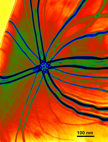
Plan view bright field transmission electron micrograph of a germanium/silicon quantum dot in a silicon matrix. The quantum dot, grown by molecular beam epitaxy, is coherently strained due to Ge/Si crystal lattice mismatches giving rise to strain induced banding contours. The straight edge at the top left shows the Si 110 plane. Field of view is approximately 620nm wide. (click to see full sized version)
Acknowledgments: Diana Zhi, Paul Midgley, Rafal Dunin-Borkowski, Don W. Pashley, Bruce A. Joyce
Visit the University of Cambridge Department of Materials Science & Metallurgy Gallery.
I will post the others in this series over time. To see it all now, visit the Nanotechnology Now Gallery.
Subscribe to:
Post Comments (Atom)


No comments:
Post a Comment