


CS2 on Au{111}
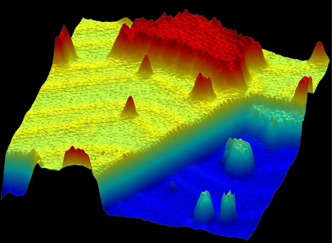
"Surfing a wave" - CS2 riding an electronic surface state on Au{111} 236 Å x 236 Å, image of 0.2 ML CS2 on Au(111) at 4 K (Vtip = + 0.5 V, I = 200 pA). (click to see larger version)
Image by: E. H. Sykes & P. Han.
"We focus on gaining atomic-scale understanding and control of materials properties. We do this by exploring, probing, and manipulating interactions and dynamics at surfaces and interfaces. We use and extend scanning tunneling microscopy to explore the surface structures, motion, and perturbations due to adsorbed atoms and molecules and due to surface features such as substrate steps and defects. We locate, study, and try to exploit the regimes in which our intuition based on macroscopic measurements breaks down. We are exploring the phenomena to be used, the ground rules, and the ultimate limits in nanometer-scale electronics and storage. Our microscopes serve not only as probes, but also allow us to manipulate matter on the atomic scale. We can thus interrogate the properties of uniquely configured atomic-scale structures. This has required the development of new tools with atomic-scale views of the surface. One new effort in our group looks at how we can bridge the gap between conventional optical microscopies and scanning probe microscopies."
~Paul S. Weiss, Professor of Chemistry, Pennsylvania State University. Weiss Group Featured Images
To see the entire series, visit the Nanotechnology Now Gallery.


No comments:
Post a Comment